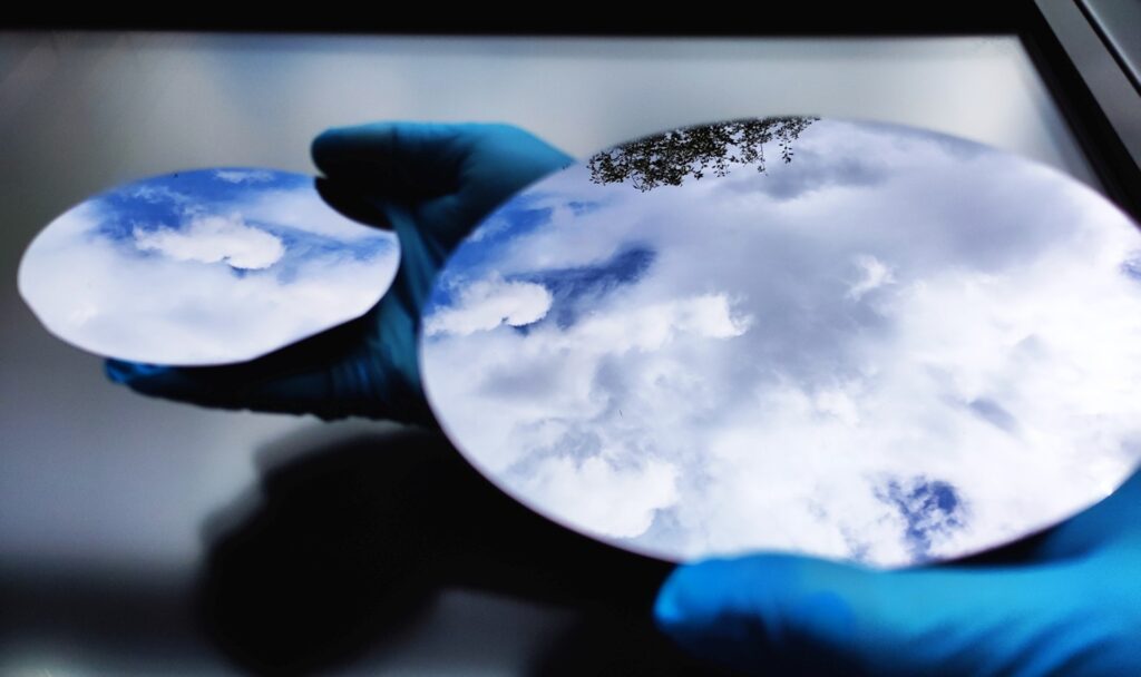
弗劳恩霍夫太阳能系统研究所的科学家们已经生产出InP-on-GaAs晶圆,直径可达150毫米。
研究团队与德国半导体专家III/V-Reclaim合作开发了一项工艺,可以在砷化镓(GaAs)上沉积一层薄薄的优质磷化铟(InP)。
该团队表示,这一应用颇具挑战性,因为磷化铟在生长过程中可能产生缺陷,从而降低最终设备的性能。为了避免这类缺陷,团队引入了一系列所谓的‘变质缓冲层’,并对完全生长的InP-on-GaAs晶圆进行了特殊的化学机械抛光处理。
经过表面处理后,晶圆表面光亮、表面粗糙度极低,且缺陷密度低于每平方厘米5*10⁶。弗劳恩霍夫太阳能系统研究所发表声明称,他们的新晶圆可以“在各种应用中有效替代传统的磷化铟,同时提供了一条具有扩展性的成本降低途径”。
弗劳恩霍夫太阳能系统研究所项目经理Carmine Pellegrino表示,公司可以使用InP-on-GaAs衬底制造高效率设备。
“但它的成本远低于磷化铟,并且可以无限扩展成直径达8英寸的晶圆。”他补充道。
该研究团队已对这些晶圆的材料质量和性能进行了测试,并与标准磷化铟衬底进行比对,测试结果“极具前景”。
Pellegrino说道:“与采用优质磷化铟晶圆制成的参考设备相比,基于我们的工程化晶圆的光伏电池实现了相当的开路电压。在整个6英寸的直径范围内,晶圆始终保持一致且均匀的性能,因此能够实现可靠的生产和高产量。”
Pellegrino指出,新衬底的生产成本显著低于磷化铟晶圆,量产时可节省多达80%的成本。
他还表示:“此外,我们的方法绕开了磷化铟供应的限制。”
This content is protected by copyright and may not be reused. If you want to cooperate with us and would like to reuse some of our content, please contact: editors@pv-magazine.com.


By submitting this form you agree to pv magazine using your data for the purposes of publishing your comment.
Your personal data will only be disclosed or otherwise transmitted to third parties for the purposes of spam filtering or if this is necessary for technical maintenance of the website. Any other transfer to third parties will not take place unless this is justified on the basis of applicable data protection regulations or if pv magazine is legally obliged to do so.
You may revoke this consent at any time with effect for the future, in which case your personal data will be deleted immediately. Otherwise, your data will be deleted if pv magazine has processed your request or the purpose of data storage is fulfilled.
Further information on data privacy can be found in our Data Protection Policy.