从Fraunhofer ISE剥离出的NexWafe公司,已获得了800万美元的融资,用于其Kerfless晶片的商业化。
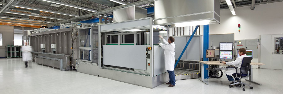
这些资金将用于NexWafe在德国弗莱堡生产基地中5兆瓦硅片生产线的调试,其目标是使产品成本降低50%,且将能源消耗也降低一半。该公司认为这一产品具有巨大的市场潜力。
公司CEOStefan Reber表示,试点生产线有望在2018年Q2完成。在试点生产线上线运行之后,该公司将寻求下一阶段的融资。他认为大规模生产设施所需的投资应该在5000-6000万欧元之间,而Kerfless硅片的众多优势,将有助于未来融资的获得。
Nexwafe的EpiWafer工艺技术,以一步主要硅沉积步骤取代了硅片生产中的四个步骤,带来了整个流程的高资源效率。
公司目前专注于硅片市场,但也将开始着眼于高效单晶硅片这一“增长最迅速的领域。”
This content is protected by copyright and may not be reused. If you want to cooperate with us and would like to reuse some of our content, please contact: editors@pv-magazine.com.







By submitting this form you agree to pv magazine using your data for the purposes of publishing your comment.
Your personal data will only be disclosed or otherwise transmitted to third parties for the purposes of spam filtering or if this is necessary for technical maintenance of the website. Any other transfer to third parties will not take place unless this is justified on the basis of applicable data protection regulations or if pv magazine is legally obliged to do so.
You may revoke this consent at any time with effect for the future, in which case your personal data will be deleted immediately. Otherwise, your data will be deleted if pv magazine has processed your request or the purpose of data storage is fulfilled.
Further information on data privacy can be found in our Data Protection Policy.